- 您现在的位置:买卖IC网 > Sheet目录3882 > PIC18F4539-I/ML (Microchip Technology)IC MCU FLASH 12KX16 EE A/D 44QFN
PIC18FXX39
DS30485A-page 18
Preliminary
2002 Microchip Technology Inc.
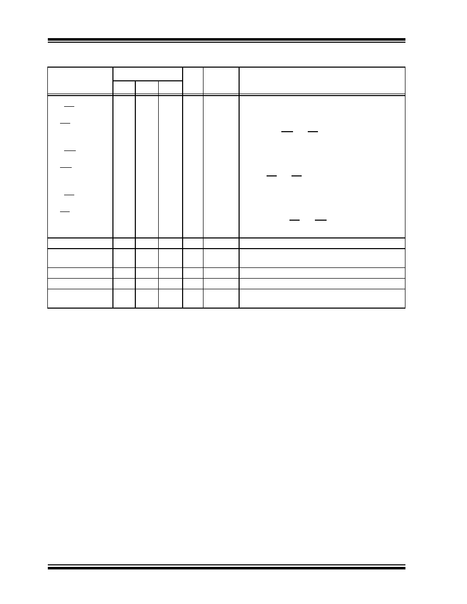
PORTE is a bi-directional I/O port.
RE0/RD/AN5
RE0
RD
AN5
8
25
I/O
ST
TTL
Analog
Digital I/O.
Read control for parallel slave port
(see also WR and CS pins).
Analog input 5.
RE1/WR/AN6
RE1
WR
AN6
9
26
I/O
ST
TTL
Analog
Digital I/O.
Write control for parallel slave port
(see CS and RD pins).
Analog input 6.
RE2/CS/AN7
RE2
CS
AN7
10
27
I/O
ST
TTL
Analog
Digital I/O.
Chip Select control for parallel slave port
(see related RD and WR).
Analog input 7.
VSS
12, 31 6, 31
6, 29
P
—
Ground reference for logic and I/O pins.
VDD
11, 32 7, 28,
29
7, 28
P
—
Positive supply for logic and I/O pins.
AVSS
—
30
—
P
—
Ground reference for analog modules.
AVDD
—
8
—
P
—
Positive supply for analog modules.
NC
—
13
12, 13,
33, 34
—
These pins should be left unconnected.
TABLE 1-3:
PIC18F4X39 PINOUT I/O DESCRIPTIONS (CONTINUED)
Pin Name
Pin Number
Pin
Type
Buffer
Type
Description
DIP
QFN TQFP
Legend: TTL = TTL compatible input
CMOS = CMOS compatible input or output
ST = Schmitt Trigger input with CMOS levels
I
= Input
O= Output
P
= Power
OD = Open Drain (no P diode to VDD)
发布紧急采购,3分钟左右您将得到回复。
相关PDF资料
PIC18F4439-I/ML
IC MCU FLASH 6KX16 EE A/D 44QFN
PIC18F2439-I/SO
IC MCU FLASH 6KX16 EE A/D 28SOIC
PIC16F687-I/SO
IC PIC MCU FLASH 2KX14 20SOIC
PIC16F877AT-I/PTG
IC MCU FLASH 8KX14 W/AD 44 TQFP
PIC16F877A-I/LG
IC MCU FLASH 8KX14 W/AD 44PLCC
PIC12LC509AT-04I/MF
IC MCU OTP 1KX12 LV 8-DFN
PIC12C509AT-04I/MF
IC MCU OTP 1KX12 8-DFN
PIC24F08KL301-I/SS
IC MCU 16BIT 8KB FLASH 20-SSOP
相关代理商/技术参数
PIC18F4539-I/P
功能描述:8位微控制器 -MCU 24KB 1408 RAM 32 I/O RoHS:否 制造商:Silicon Labs 核心:8051 处理器系列:C8051F39x 数据总线宽度:8 bit 最大时钟频率:50 MHz 程序存储器大小:16 KB 数据 RAM 大小:1 KB 片上 ADC:Yes 工作电源电压:1.8 V to 3.6 V 工作温度范围:- 40 C to + 105 C 封装 / 箱体:QFN-20 安装风格:SMD/SMT
PIC18F4539-I/P
制造商:Microchip Technology Inc 功能描述:IC 8BIT FLASH MCU 18F4539 DIP40
PIC18F4539-I/PT
功能描述:8位微控制器 -MCU 24KB 1408 RAM 32 I/O RoHS:否 制造商:Silicon Labs 核心:8051 处理器系列:C8051F39x 数据总线宽度:8 bit 最大时钟频率:50 MHz 程序存储器大小:16 KB 数据 RAM 大小:1 KB 片上 ADC:Yes 工作电源电压:1.8 V to 3.6 V 工作温度范围:- 40 C to + 105 C 封装 / 箱体:QFN-20 安装风格:SMD/SMT
PIC18F4539IPT
制造商:MICRO CHIP 功能描述:NEW
PIC18F4539T-E/ML
功能描述:8位微控制器 -MCU 24KB 1408 RAM 32 I/O RoHS:否 制造商:Silicon Labs 核心:8051 处理器系列:C8051F39x 数据总线宽度:8 bit 最大时钟频率:50 MHz 程序存储器大小:16 KB 数据 RAM 大小:1 KB 片上 ADC:Yes 工作电源电压:1.8 V to 3.6 V 工作温度范围:- 40 C to + 105 C 封装 / 箱体:QFN-20 安装风格:SMD/SMT
PIC18F4539T-E/PT
功能描述:8位微控制器 -MCU 24KB 1408 RAM 32 I/O RoHS:否 制造商:Silicon Labs 核心:8051 处理器系列:C8051F39x 数据总线宽度:8 bit 最大时钟频率:50 MHz 程序存储器大小:16 KB 数据 RAM 大小:1 KB 片上 ADC:Yes 工作电源电压:1.8 V to 3.6 V 工作温度范围:- 40 C to + 105 C 封装 / 箱体:QFN-20 安装风格:SMD/SMT
PIC18F4539T-I/ML
功能描述:8位微控制器 -MCU 24KB 1408 RAM 32 I/O RoHS:否 制造商:Silicon Labs 核心:8051 处理器系列:C8051F39x 数据总线宽度:8 bit 最大时钟频率:50 MHz 程序存储器大小:16 KB 数据 RAM 大小:1 KB 片上 ADC:Yes 工作电源电压:1.8 V to 3.6 V 工作温度范围:- 40 C to + 105 C 封装 / 箱体:QFN-20 安装风格:SMD/SMT
PIC18F4539T-I/PT
功能描述:8位微控制器 -MCU 24KB 1408 RAM 32 I/O RoHS:否 制造商:Silicon Labs 核心:8051 处理器系列:C8051F39x 数据总线宽度:8 bit 最大时钟频率:50 MHz 程序存储器大小:16 KB 数据 RAM 大小:1 KB 片上 ADC:Yes 工作电源电压:1.8 V to 3.6 V 工作温度范围:- 40 C to + 105 C 封装 / 箱体:QFN-20 安装风格:SMD/SMT